How They’re Made
From the world’s most advanced manufacturing comes the world’s most advanced technology—where cutting-edge techniques, equipment, and analysis are controlled with atomic-level precision.
Tomorrow’s technology begins in a fab
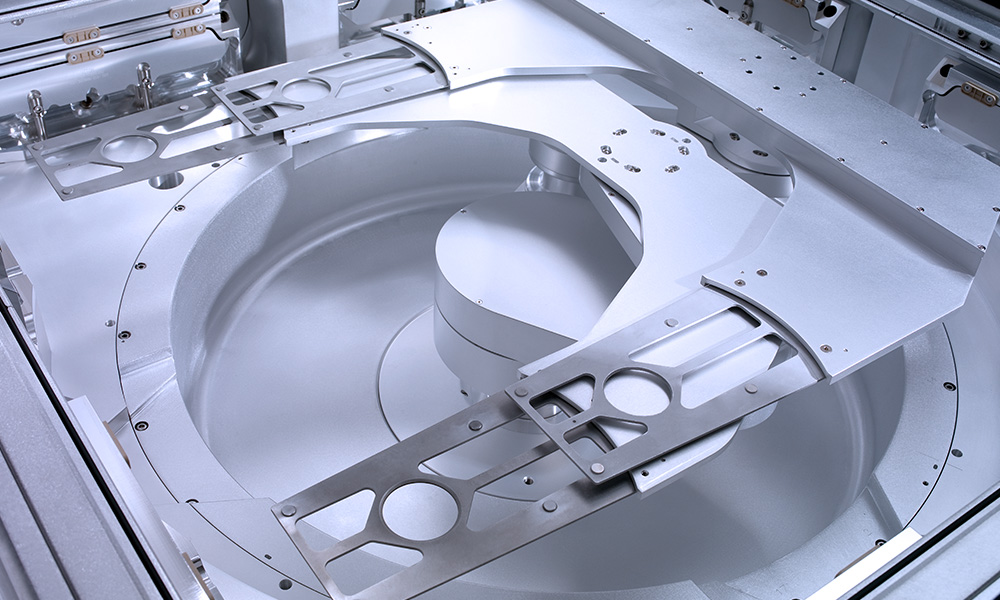
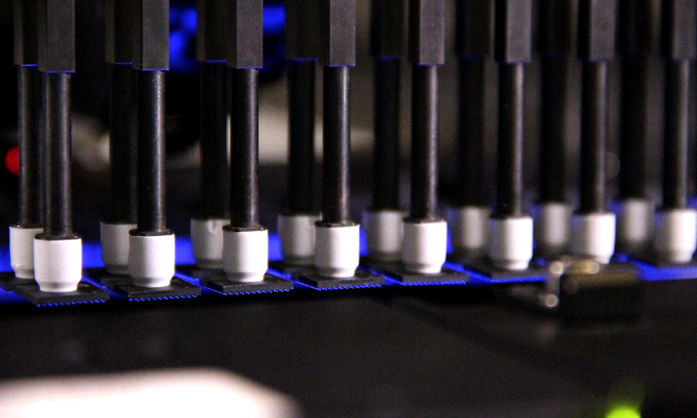
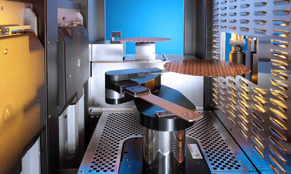
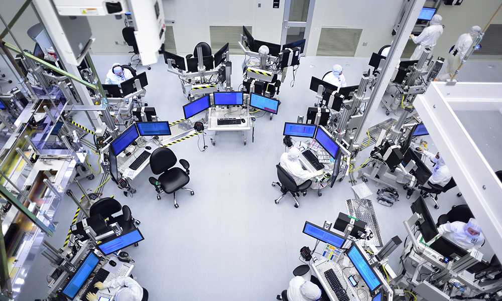
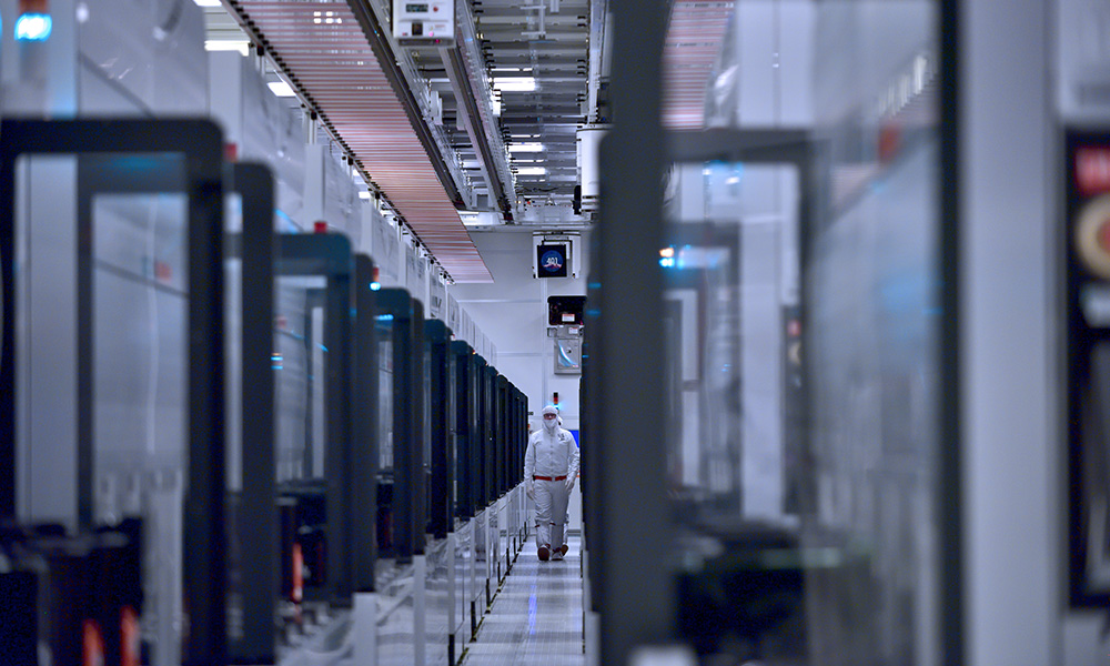
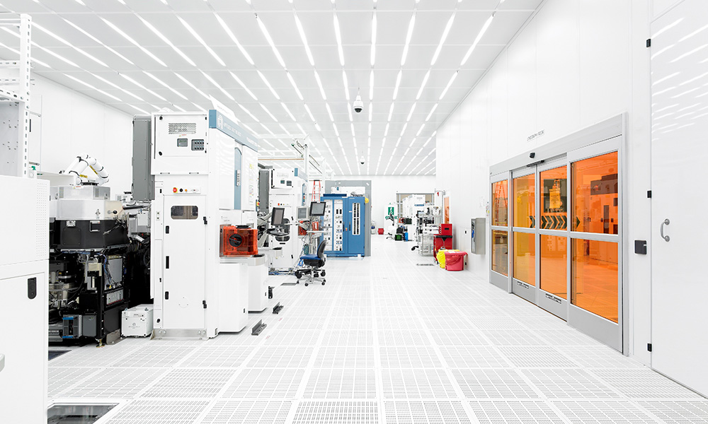
Technically speaking, a semiconductor fab (short for fabrication plant) is a manufacturing facility where microchips are made. But it’s actually the most breathtaking symphony of coordinated production imaginable—with thousands of process machines running plasmas, lasers, ultra-precision optics, ion accelerators, and advanced robotics—all synchronized to crank out hundreds of thousands of wafers, each containing hundreds, even thousands, of chips.
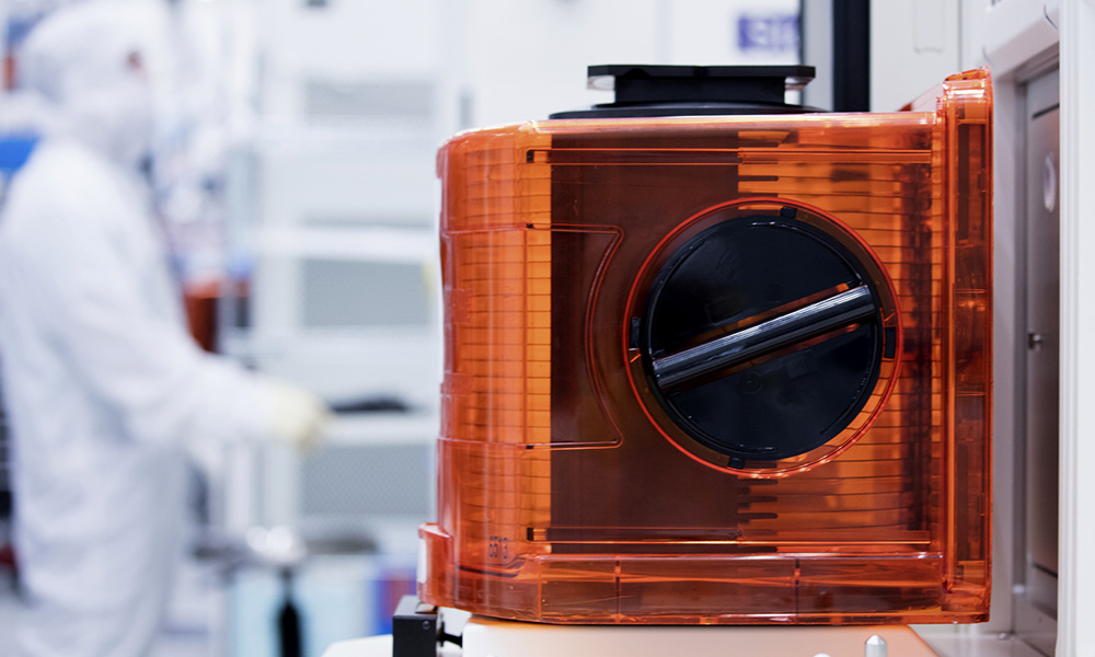
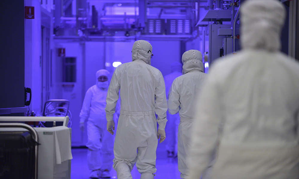
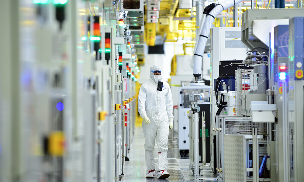
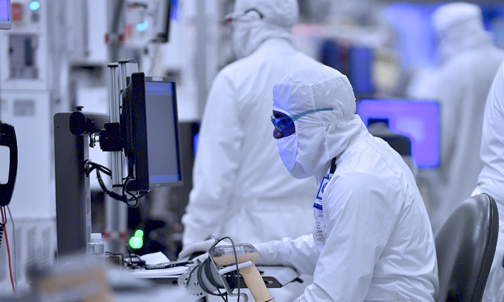
Taking center stage in a fab is the clean room—with the emphasis on clean—since a single microscopic particle the size of a virus can ruin a microcircuit.
$15–20 BILLION1
Cost of a leading-edge fab by 2020
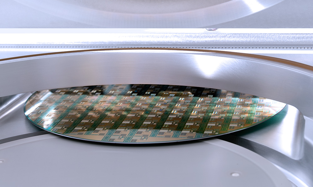
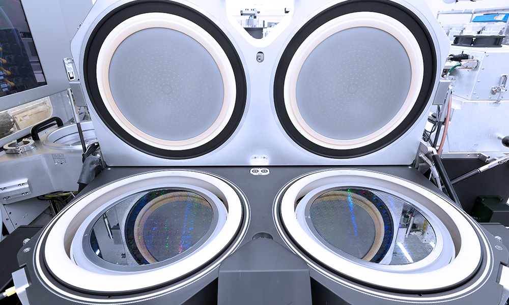
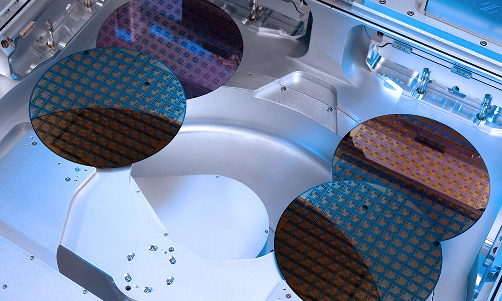
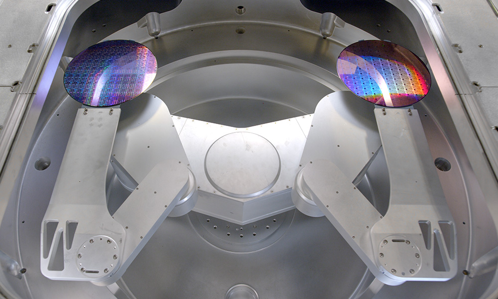
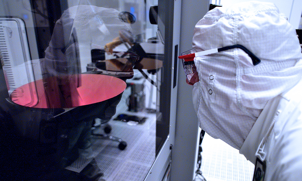
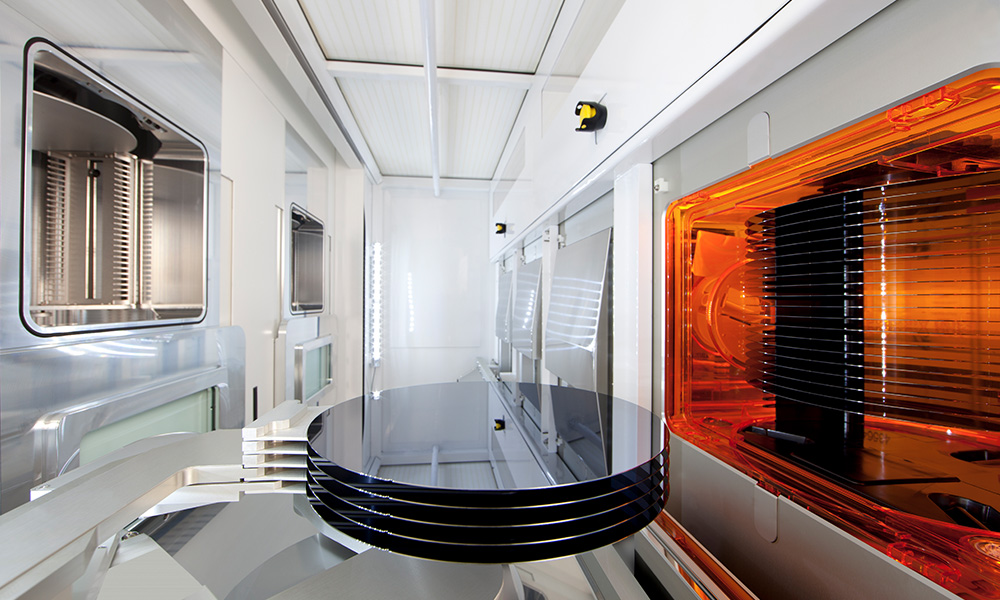
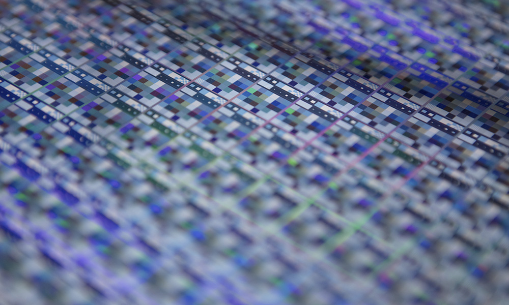
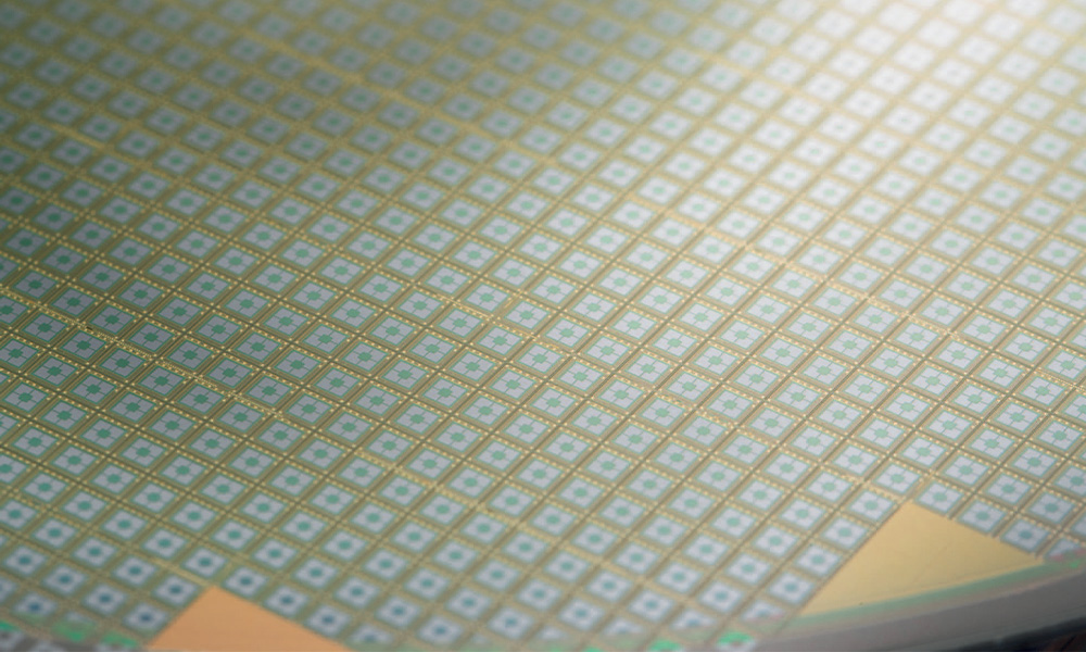
Silicon wafers: the indispensable foundation of all semiconductors
Silicon wafers are ultra-thin discs of pure, single-crystal, polished silicon that serve as the foundation microchips are built on. Every wafer is built from stacks of the thinnest films imaginable—each patterned to form transistors and microcircuits before being cut into individual computer chips.
Because electrical currents are much easier to control when passed through silicon than other materials, these wafers are vital to the function of chips, where the need for speed is of the essence. Yes, silicon may be the second-most common element on Earth (after oxygen), but it’s an uncommonly important substance.
Who knew manufacturing could actually be inspiring?
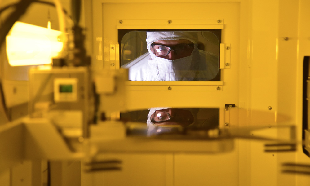
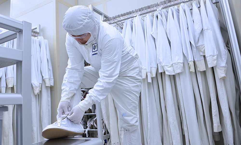
Until you’ve put on a “bunny suit,” passed through an “air shower” to remove any extraneous particles, and walked inside a fab, it’s hard to imagine just how complicated it is to make microchips. It means packing hundreds, millions, or billions of transistors onto a fingernail-sized area of silicon wafer using some of the world’s most sophisticated (and expensive) instruments.
Each step in the process happens at a microscopic level, building three-dimensional structures that can include up to 90 layers of complex circuitry.
100,000x2
How much more sterile a clean room can be compared to a hospital operating room
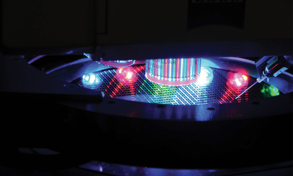
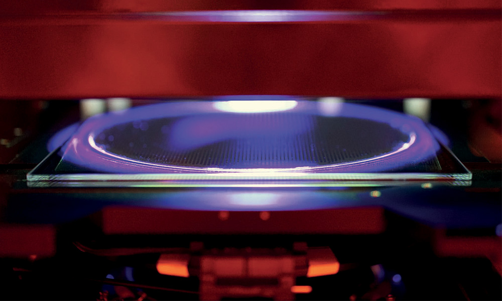
INSIDE THE FAB
Here’s a glimpse of the highly advanced facilities, people, and equipment our SEMI member companies use to create the semiconductors you use every day.


Load more
1 EE Times, 2012
2 OR Today, 2012
2 OR Today, 2012